Product of Melfas
We introduce you to MELFAS, a leading touch input solution market company.
Home > Technologies & Products > Products


-
Product Information
MFP - Melfas Finger Printer
■ Product Introduction
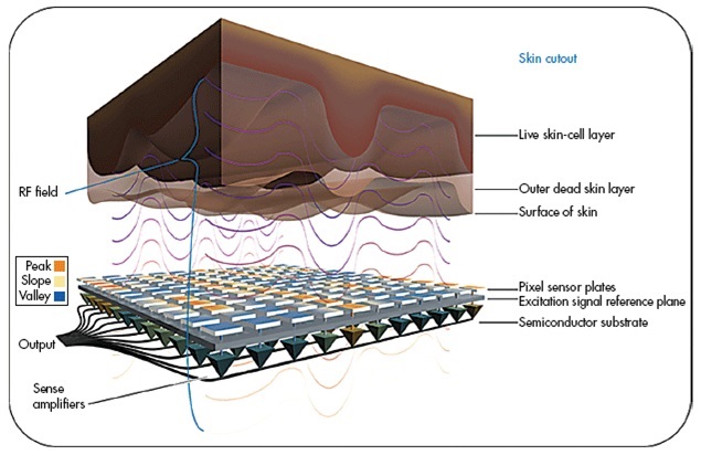
The fingerprint sensor is the input image device which obtains the image information of the fingerprint that shows the unique characteristics individually. It judges with the secured primitive fingerprint image whether it is the person after comparing and matching it to the characteristic information of the users already registered in the database after extracting the features of the fingerprint.
This kind of the fingerprint system is divided into the hardware sensor part which obtains the images and the software algorithm part which analyzes the obtained image information and recognizing the fingerprint. The fingerprint images are obtained in various methods including semiconductor element method which detects the capacitance or the electrical conduction, ultrasonic wave method, thermal method, non-contact method, or the combination of these methods. The capacitance-type fingerprint sensor of the semiconductor method recognizes the difference of the capacitance according to the patterns of the valley and ridge of the fingerprints and then obtains the fingerprint image using the sensing array which is materialized in the uppermost layer of the semiconductor chip.
The size of the individual sensing electrode is determined according to the resolution of the fingerprint image, usually, the resolution of the image to secure the stability of the fingerprint system is at least more than 300dpi, and the sensing array is materialized with the very fine gaps among the electrodes below 100um.
To detect the change of the capacitance by the fingerprint pattern, the sensing circuit with a very good sensitivity needs to be embodied. Systematically, the closer the distance between the surface of the sensor and the contact part of the finger print is, the more advantage of the sensing sensitivity. Because the characteristics degradation occurs such as the durability and ESD which are required during the SMT on the set, the improvement of the sensitivity through the circuit is the best method. With this, the bigger the fingerprint image is, the more information of the characteristics of the fingerprint can be obtained, which leads to the stable fingerprint recognition rate. Thus, this makes the manufacturing cost increase due to the bigger size of the semiconductor chip.
Along with this, even to make the cost lower by reducing the size of the chip, the additional fingerprint characteristic information instead of the basic fingerprint characteristic information which is generally used needs to be made and then the fingerprint recognition rate needs to be secured even in the smaller area. In this case, too, the acquisition of the fingerprint image information of the three- dimension through the high-sensitivity circuit is necessary.
-
Applicable Products
-